Add a thermal interface layer
Use a zero-thickness cuboid with the conducting_surface thermal model to represent a thin thermal interface material (TIM), such as a pad or paste layer between a package and a heatsink. This adds resistance to heat flow across the interface without requiring mesh cells small enough to resolve the layer’s thickness.
Place the interface
Position the adjacent components so that their contact faces meet at the same plane. Add a new object to cuboid_components with a unique tag, and set exactly one dimension of its bbox.size to zero. The other two dimensions define the contact area.
For example, the following surface covers a 30 mm by 20 mm contact in the plane z = 0.013 m. Merge it into your existing cuboid_components list:
{
  "tag": "tim",
  "bbox": {
    "origin": [0.04, 0.02, 0.013],
    "size": [0.03, 0.02, 0.0]
  },
  "thermal_model": {
    "conducting_surface": {
      "thickness": 0.0001,
      "conductivity": 3.0
    }
  }
}
Here, the lower component’s top face and the upper component’s bottom face should both lie at z = 0.013 m. Keep them touching rather than leaving a fluid gap for the TIM. The surface’s thickness is a thermal-model input; it does not expand the bounding box or separate the components.
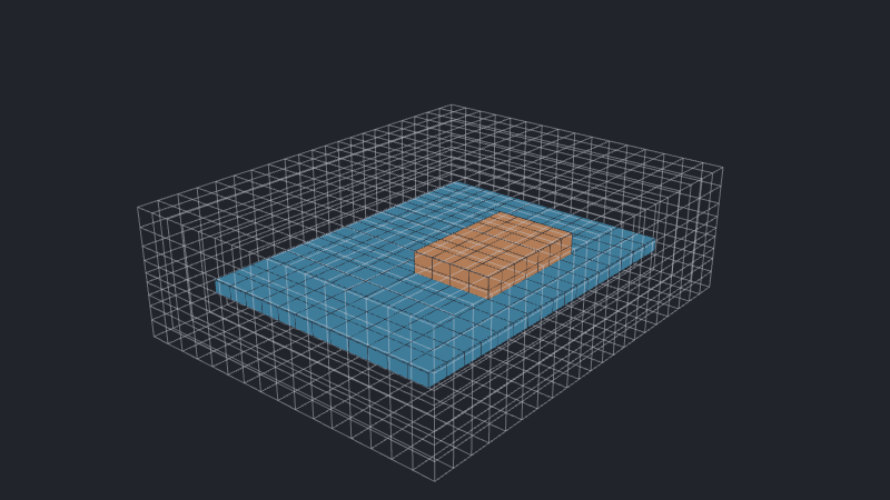
Compare the two TIM representations below. Both use the same chip and board dimensions and mesh settings. The explicit layer raises the chip by 0.1 mm to accommodate its physical thickness; the surface keeps the components touching.
Set the layer’s properties
Supply a positive thickness in meters and a positive conductivity in \(\mathrm{W/(m\,K)}\). The example represents a 0.1 mm layer with conductivity \(3\,\mathrm{W/(m\,K)}\).
The layer models conduction normal to its plane. Use a volumetric conducting component if you need to resolve temperature variation or heat spreading within the layer. No additional thermal boundary condition is needed to connect two conducting regions through this surface. Conducting surfaces explains the resistance model.
Place a layer over a thermal boundary
You can also align the layer with an existing thermal boundary on a domain wall or an insulating component’s face. Supported conditions are fixed_temp, fixed_htc, heat_flux, and adiabatic. Keep the condition on the original boundary; Vanellus automatically accounts for the layer over the covered area. See Surfaces over thermal boundaries for how each condition is affected.
Place a layer on a compact thermal model
Use the same conducting_surface object directly on an active CTM face. For example, if a chip’s case_side is z_max and its top face is at z = 0.013 m, place the cold plate’s bottom at that same height and use the TIM object above to cover their contact. This gives the stack CTM → TIM → cold plate, with no extra solid layer or fluid gap.
Keep the CTM’s package resistances unchanged; meshing adds the TIM resistance to the corresponding solver-side package resistance and absorbs the covered surface footprint. The case and board faces of both two-resistor and STAR CTMs support TIMs; the other four STAR faces do not. Each layer must cover every active CTM face it overlaps completely. A larger layer is allowed, including one spanning several complete CTM faces; partial coverage of any active face is rejected. Any overhang retains the ordinary conducting-surface behavior, including acting as a wall where it touches fluid. The complete active CTM face must still touch fluid or conducting solids.
See also
- Add a cuboid component covers volumetric components and insulating surfaces.
- Conducting surfaces explains the surface thermal model.
- Conducting and insulating domains explains which regions participate in the temperature solve.
- Configure the mesh explains refinement and geometry preservation.